The AD9059is a dual 8-bit single-chip analog-to-digital converter optimized for low cost, low power, small size and ease of use. With a typical MS MS encoding rate of 60 MSPS and a full-power analog bandwidth of 120 MHz, this component is ideal for applications that require multiple ADCs with excellent dynamics.
To minimize system cost and power consumption, the AD9059 includes an internal 2.5 V reference and dual-channel keeper circuitry. The ADC requires only a 5 V supply and an encoding clock. Many applications are not required for external reference or driver components.
The single-encoded input of the AD9059 is TTL/CMOS compatible and controls both internal ADC channels. This parallel 8-bit digital output can be used to operate at 5 V or 3 V. The power-down function can be performed without ADC data, and the total power consumption is <12 mW for a long time. In power save mode, the digitized output is driven to a high impedance state.
The AD9059 is fabricated in an advanced BiCMOS process in a space-saving 28-lead shrink small outline package (28-pin SSOP) and is specified over the industrial temperature range (-40°C to + 85°C). Customers who want single-channel digitization can consider using
The AD9057 is based on a single 8-bit, 60 MSPS microcontroller AD9059 ADC core. The AD9057 is available in a small package of 20-pin shrink devices (20-pin SSOP) and specified over the industrial temperature range.
feature:
Dual 8-bit ADC on a single chip
Low power: 400 mW typical
On-chip 2.5 V reference and tracking hold
1 V p-p analog input range
Single 5V power operation
5 V or 3 V logic interface
120 MHz analog bandwidth
Power-down mode: <12 mW
application:
Digital communication (QAM demodulator)
RGB and YC / composite video processing
Digital data storage read channel
Medical Imaging
Digital instrument
Functional block diagram:

PIN configuration diagram:

Operational theory:
The AD9059 combines Analog Devices' proprietary MagAmp gray code conversion circuitry with flash converter technology to provide dual high performance 8-bit ADC monolithic devices at low cost. The design architecture ensures low power, high speed, and 8-bit accuracy.
The AD9059 provides two clocked linked ADC channels from a single ENCODE input (see the functional block diagram). Two ADC channels simultaneously sample analog inputs (AINA and AINB) and provide non-interlaced parallel numbers
Output (D0A-D7A and D0B-D7B). The voltage reference (VREF) is internally connected to both ADCs, so the channel gain and offset will track if external reference control is required. The analog input signal buffers the channel at the input of each ADC and is applied to high speed tracking and hold. The track and hold circuit maintains the analog input value conversion process (starting from the rising edge) during the hold period. ENCODE command). The tracked and held output signals are generated by the Gray code and flash conversion stages to generate a coarse and fine digital representation level of the held analog input. The decode logic combines multiple levels of data and aligns the strobe output of the rising edge of ENCODE to an 8-bit word command. The AD9059's MagAmp / Flash architecture results in three pipeline delays in the output data. Using the AD9059
The analog input AD9059 provides a separate single-ended, high-impedance (150kΩ) analog input for dual ADCs. Each input requires a DC bias current of 6μA (typ) and a center close to 2.5V (±10%). This DC offset can be provided by the user or can be derived from the internal reference voltage of the ADC. The figure below shows that low-cost DC allows the user to capacitively couple the bias to allow the AC signal to go directly into the ADC without the need for additional active circuitry. For best dynamic performance, the VREF pin should be decoupled to ground with a 0.1μF capacitor (to minimize the modulation reference voltage) and the bias resistor should be approximately 1kΩ.
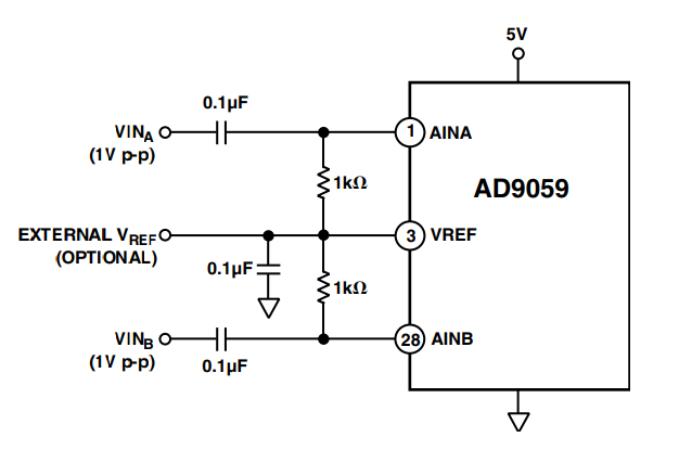
Capacity coupling AD9059:
The figure below shows a typical connection for high performance DC with the ADC's internal reference voltage for biasing. All components can be powered from a single 5V supply (analog input signals are referenced to ground).

DC coupled AD9059 (VIN inverting)
Voltage reference:
Built-in stable, accurate 2.5 V reference AD9059 (VREF). The reference output is used to set the ADC gain/offset to provide a DC offset for the analog input signal. The internal reference is capable of providing 300μA of current external drive current (for DC bias analog input or other user circuits) through an 800Ω internal impedance connected to the ADC circuit. Some applications may require higher quasi-temperature performance, or gain adjustments that cannot be made using internal references. An external voltage may be applied to the VREF pin to overdrive the internal voltage gain adjustment reference up to ±10% (the VREF pin is internally tied directly to the ADC circuit). The ADC gain and offset will vary simultaneously with the external reference adjustment at a 1:1 ratio of 2% or 50 mV for 2.5 V. The reference increases the ADC gain by 2% and the ADC offset by 50 mV).
Digital Logic (5 V / 3 V System)
The digital inputs and outputs of the AD9059 can be easily configured to interface directly to a 3 V or 5 V logic system. The code and power-down (PWRDN) inputs are CMOSTTL thresholds of 1.5 V, making the inputs compatible with TTL, 5 V CMOS and 3 V CMOS logic families. For all high speed data converters, the encoded signal should be clean and jittered to prevent ADC dynamic degradation performance.
The digital output of the AD9059 can also be used directly with a 5 V interface or a 3 V CMOS logic system. The power supply pin (VDD) is used to isolate these CMOS stages from the analog VD voltage supply. By changing the voltage on these power pins, the digitization will change for a 5 V or 3 V system. The VDD pin is internally connected to the AD9059 chip. Caution should be used to isolate the 5V supply voltage and the 5 V analog voltage supply to minimize noise coupled to the ADC.
The AD9059 provides a high impedance digital output operation when the ADC enters power-down mode (PWRDN, logic high). It should be 200 ns (minimum) power down time provided before high impedance characteristics are required. One provides 200 ns of power-up time to ensure accurate ADC output data after reactivation (effective output data is available for three clock cycles after a 200 ns delay). The timing AD9059 guarantees operation from 5 MSPS to 60 MSPS at conversion rate. At 60 MSPS, the ADC is designed to operate with a 50% coded duty cycle, but performance is not sensitive to moderate variations. A pulse width variation of ±10% (allowing the encoded signal to meet the minimum/maximum high/low specifications) will not result in degraded ADC performance. Because the ADC's ENCODE architecture is interrelated, the AD9059 cannot run in two-channel ping-pong mode. Power Consumption The power consumption of the AD9059 is specified to reflect a typical application setting under the following conditions: coded at 60 MSPS, analog input is -0.5 dBFS at 10.3 MHz, VD is 5 V, VDD is 3 V, typical digital output It is 7 pF (up to 10 pF). The actual dissipation therefore varies the condition in the user application. TPC 7 shows the typical power consumption frequency and VDD supply voltage of the AD9059 and ADC code. The power-saving feature allows the user to reduce power consumption when ADC data is not needed. The TTL / CMOS high signal (PWRDN) turns off the part of the dual ADC and brings the total power consumption to less than 10 mW. The internal bandgap power reference remains active during power-down mode to minimize ADC reactivation time. If the power-down feature is not desired, pin 3 should be grounded. Both ADC channels are controlled simultaneously by the PWRDN pin; they cannot be turned off or turned on independently.
application:
The wide analog bandwidth of the AD9059 makes it attractive for a variety of high performance receiver and encoder applications. The figure below shows a typical low cost I and Q dual ADC wired, satellite or wireless demodulator implementing a LAN modem receiver. Excellent dynamic performance ADC with high analog input frequency and encoding rate allows users to use direct IF sampling technology. IF sampling eliminates or simplifies the analog mixer and filtering stages to reduce overall system cost and power.

The AD9059's high sample rate and analog bandwidth are ideal for computer RGB video digitizer applications. With full power analog bandwidth for up to 2x the maximum sample rate, the ADC provides enough pixel-to-pixel transient settling time to ensure accurate 60 MSPS video digitization. The figure below shows a typical RGB video to digital converter implementation of the AD9059.

The AD9059 / PCB evaluation board is easy to use for analog/digital interfaces for dual, 8-bit, 60 MSPS ADCs. The board includes a variety of high-level typical hardware configuration acceleration digital evaluations. On-board components include the AD9059 (in a 28-pin SSOP package), optional analog input buffer amplifiers, digital output latches, board timing drivers, and configurable jumpers for AC-coupled, DC-coupled, and power-down functional tests. The board is factory configured to use the internal reference of the AD9059 for DC coupling. For DC-coupled analog input applications, amplifiers U3 and U4 are configured as an offset of the adjustable unity-gain inverter analog input signal. For full-size ADC drives, each analog input signal should be 1 V p-p, reference 50Ω to ground. Each amplifier shifts its analog signal + VREF (typically 2.5 V) to center the voltage for the correct ADC input drive. For DC-coupled operation, connect E7 to E9 (analog inputs A through R11), E14 to E13 (amplifier output to analog input A) AD9059), E4 to E5 (analog inputs B to R10), and E11 to E10 (use the board) Output the amplifier to the analog input B) jumper connector of the AD9059. For AC-coupled analog input applications, amplifiers U3 and U4 are removed from the analog signal path. The analog signal is coupled through capacitors C11 and C12, each terminated by a separate 1kΩ resistor to provide the VREF voltage (providing the bias current of the AD9059 analog input, AINA and AINB).
The board's analog input signal should be 1 V p-p to 50Ω for full-scale ADC drive. For AC-coupled operation, connect E7 to E8 (analog input A to C12 punch-through capacitors), E13 to E15 (channel A to C12 to R15 termination resistors), E4 to E6 (analog input B to C11 pass-through capacitors) and E10 to E12 (C11 to R14 terminating resistor for channel B) uses a board jumper connector. The onboard reference voltage can be used to drive the ADC or an external reference can be applied. The standard configuration uses an internal voltage reference without any external voltage connection requirements. The external reference voltage can be a current output applied to the board connector input REF to overload limit the internal reference voltage of the AD9059. This external reference should be 2.5 V typical. You can use the power-down feature of the AD9059 to connect through the board jumper. Connect E2 to E1 (5 V to PWRDN) for power-down mode operation. For normal operation, connect E3 to E1 (grounded to PWRDN).
The coded source should be TTL/CMOS compatible and capable of driving a 50Ω termination. Digital Output During evaluation, the AD9059 uses a latch for the buffer boards (U5 and U6) that are available to the connector user using pins 30-37 and pins 22-29. The latch timing is derived from providing the ADC ENCODE clock and digital clock signals to the board users at connector pins 2 and 21.