Understanding GaN in one article: Nanomicro's most comprehensive introduction, taking you to get to know the third-generation semiconductor quickly
What is gallium nitride (GaN)?
Gallium nitride is a compound that combines gallium (atomic number 31) and nitrogen (atomic number 7). It is a wide band gap semiconductor material with a stable hexagonal crystal structure. The band gap refers to the energy required for electrons to escape from the nuclear orbit. The band gap of gallium nitride is 3.4 eV, which is more than three times that of silicon, so gallium nitride has a wide band gap (WBG).
The forbidden band width determines the electric field that a material can withstand. Gallium nitride has a larger band gap than traditional silicon materials, so it has a very narrow depletion region, so that a device structure with a very high carrier concentration can be developed. Due to the advantages of GaN with smaller transistors, shorter current paths, and ultra-low resistance and capacitance, the charging devices of GaN chargers operate 100 times faster than traditional silicon devices.
More importantly, compared to traditional silicon, GaN can handle a larger electric field in a smaller device space while providing faster switching speeds. In addition, gallium nitride can operate at higher temperatures than silicon-based semiconductor devices.

To
Why is gallium nitride (GaN) important?
The importance of gallium nitride (GaN) has become increasingly prominent and increasing. Because compared with traditional silicon technology, it not only has excellent performance and a wide range of applications, but also can effectively reduce energy loss and space occupation. In some R&D and applications, traditional silicon devices have reached their physical limits in terms of energy conversion. Gallium nitride with a higher upper limit can organically unify the advantages of charging efficiency, switching speed, product size and heat resistance, and is naturally more popular.
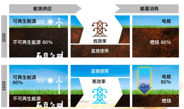
With the continuous increase of global energy demand, the use of gallium nitride technology can not only meet the energy demand, but also effectively reduce carbon emissions. In fact, the design and integration of GaN has been proven to serve as a next-generation power semiconductor, and its carbon footprint is 10 times lower than that of traditional silicon-based devices. It is estimated that if the global data centers using silicon chip devices are upgraded to use gallium nitride power chip devices, then the global data centers will reduce energy waste by 30-40%, which is equivalent to saving 100 MWh of solar energy and 1.25 Billion tons of carbon dioxide emissions.
The appeal of GaN is not only the improvement in performance and energy efficiency at the system level. When we discovered that manufacturing a single piece of gallium nitride power chip, it can reduce 80% of the chemical and energy consumption in the manufacturing process. In addition, it can save more than 50% of packaging materials. The environmental advantages of gallium nitride will be far Much larger than traditional slow silicon materials.
Gallium Nitride: History and Future
Gallium does not exist as an element in nature. It is usually a by-product produced in the process of processing bauxite into aluminum, or the process of refining sphalerite into zinc. Therefore, the carbon footprint of gallium extraction and refining is very low.
The annual output of gallium exceeds 300 tons, and the world's storage capacity is expected to exceed 1 million tons. Since gallium is a by-product of processing, the cost is relatively low, about US$300 per kilogram, which is 200 times lower than gold, which is about US$60,000 per kilogram.
Dmitri Mendeleev predicted the existence of gallium in 1871. In 1875, Paul-Émile Lecoq de Boisbaudran (Paul-Émile Lecoq de Boisbaudran) discovered gallium in Paris, and named it after his native French Latin, Gallia (Gaul). The melting point of pure gallium nitride is only 30 degrees Celsius (86 degrees Fahrenheit), so at normal body temperature, it will melt in a human hand.
After another 65 years, GaN was synthesized artificially for the first time. It was not until the 1960s that the technology for manufacturing gallium nitride single crystal thin films emerged. As a compound, gallium nitride has a melting point of over 1600°C, which is 200°C higher than silicon.
In 1972, LED light-emitting diodes based on gallium nitride material were invented (using gallium nitride doped with magnesium). This is a landmark historical event. Although the original GaN LEDs were not bright enough for commercial use, this is the first time that humans have produced LEDs that can emit blue-violet light. In 1991, a method of producing higher-brightness blue LEDs was patented, and two years later, high-brightness blue LEDs were born.
Commercial use of high-brightness blue LEDs is a turning point in the electronics industry. By adding phosphor coatings, humans have realized that it is possible to create white LEDs that can replace low-efficiency incandescent lamps. Add red and green LEDs to form an LED-based display. From the first LED-backlit LCD TV to the latest OLED screen, this has accelerated the replacement of the cathode ray tube (CRT) TV and display market, and the demise of silicon-based "deflection transistor" screen products.
Therefore, GaN is the core technology behind the high-resolution color screens we use in TVs, mobile phones, tablets, laptops, and monitors. In terms of photonics, gallium nitride is also used in blue laser technology (most notably the optical disc laser head used in Blu-ray players).
In addition to photonics, although gallium nitride transistors released related technologies in 1993, it was not until around 2004 that the first gallium nitride high electron mobility transistor (HEMT) began to be commercially available. These transistors are commonly used in radio frequency infrastructure that requires high performance and high voltage. A few years later, in 2008, GaN metal oxide semiconductor field effect crystals (MOSFETs) (formed on silicon substrates) were promoted, but due to complex circuits and lack of high-frequency ecosystem components, the utilization rate was low.
Founded in 2014, Nanomicro Semiconductor's mission is to give full play to the advantages of wide bandgap devices of GaN power chips in a wide range of applications, deliver the broad possibilities of wide bandgap technology applications, and realize a speed revolution in the field of power electronics. In 2018, Nanomicro Semiconductor was selected as EETIMes’s famous "Silicon 60" startup company list. In 2019, Frost and Sullivan Frost and Sullivan recognized the unique vision, system solutions and core technologies of Nanomicro Semiconductor. It is believed that Nanomicro is expected to spawn and bring next-generation power systems based on gallium nitride. In the same year, Nanomicro Semiconductor was awarded the title of "Innovation Star" by Shanghai Zhangjiang 895 and Zhangjiang Science City ICV Pioneer Alliance. Subsequently, in 2020, Nanomicro Semiconductor also won the "Semiconductor Design Innovation Excellence Award" and the China Communications Industry Association (CCIA). "Aspencore Outstanding Innovative Company of the Year" award.

Also in 2020, Nanomicro Semiconductor announced more than 100 patents for GaN devices and applications.
Nanomicro Semiconductors continues to continue to develop GaNFast series of power chip products. Unlike most traditional silicon devices or early discrete GaN devices, these devices of Nanomicro Semiconductors use a very small surface mount package QFN, which eliminates the speed-limiting and detrimental discrete drive and protection circuits, and Reduce the printed circuit board (PCB) area.
As of April 1, 2021, Nanomicro Semiconductors has completed the shipment and transportation of 18.2 million zero-fault gallium nitride power chips.
If you need to check the latest GaN power chip shipment and quality information, please visit our product quality page.
Applications of GaN
For a long time, gallium nitride has been used in the production of LEDs and radio frequency components, but now, in the ever-growing power switch and conversion application market, gallium nitride has increasingly become the mainstream choice. And the power chip based on gallium nitride can also meet the requirements of high performance, small space occupation, and high temperature resistance.
In mobile phones and laptops, you can use GaN-based radio frequency devices to send and receive mobile network and WiFi signals. The chargers that charge these devices are increasingly using gallium nitride power chips. Currently, the largest market for power GaN is the fast charging market for mobile devices. The gallium nitride power chip can make the charging speed of the charger three times faster than the traditional silicon charger, but the size and weight are only half of the latter. More importantly, the single-port charger products using GaN are only half the price of the old best old silicon chargers; and the multi-port GaN chargers are more expensive than the old old silicon chargers. The device is more than three times lower.

Gallium nitride power chips can also be deployed in data center servers. With the increase in data center traffic, the ability of silicon to transmit energy has reached the limit of "physical properties". Eventually, traditional silicon chips will be replaced by high-speed gallium nitride power chips in the field of power chips.
The integration of data center hardware, the new HVDC high-voltage DC architecture method, and the mass-produced, highly integrated gallium nitride power chip have greatly improved the charging efficiency. It is estimated that if the global data centers using silicon devices are upgraded to gallium nitride devices, the global data centers will reduce energy waste by 30-40%, which is equivalent to saving 100 MWh of solar energy and 125 million tons Carbon dioxide emissions. Therefore, the use of gallium nitride represents another solid step towards the goal of "Net-Zero" in the data center industry.

In the automotive industry, GaN is becoming the preferred technology for power conversion and battery charging in the field of new energy vehicles. GaN-based power products are also increasingly appearing in inverters used in solar power generation devices, as well as in motor drives and other industrial power conversion solutions.
Why is gallium nitride better than silicon?
Gallium nitride (GaN) is a "wide band gap" (WBG) material. The band gap refers to the energy required for electrons to escape from the nuclear orbit. The band gap of gallium nitride is 3.4ev, which is more than three times that of silicon, so gallium nitride has a wide band gap (WBG).
The band gap of silicon is 1.1 eV, and the band gap of gallium nitride is 3.4 eV. Because the wide band gap material has high electric field strength and the depletion region is narrow and short, a device structure with a very high carrier concentration can be developed. For example, a typical 650V lateral gallium nitride transistor can support a voltage exceeding 800V, and its drain drift region is 10-20μm, or about 40-80V/μm. This is much higher than the theoretical limit of 20V/μm for silicon. However, GaN devices are still far below the band gap limit of about 300V/µm, which leaves huge room for future optimization and improvement.
At the device level, according to the actual situation, the figure of merit obtained by the product of the normalized on-resistance (RDS (ON)) and the gate charge (QG) is 5 to 20 times better than that of silicon. By using smaller transistors and shorter current paths, GaN chargers will be able to achieve ultra-low resistance and capacitance, and the switching speed can be increased by a hundred times.
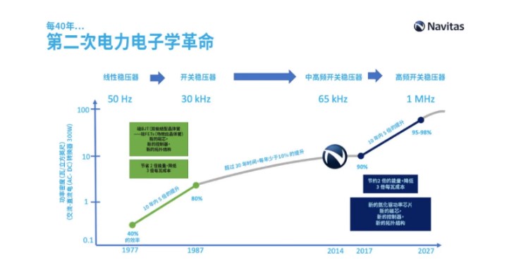
In order to take full advantage of the capabilities of GaN power chips, other parts of the circuit must also operate efficiently at higher frequencies. After adding the control chip in recent years, the switching frequency of the GaN charger has been increased from 65-100kHz to above 1MHz. The new controller is under development. Microcontrollers and digital signal processors (DSP) can also be used to implement current soft-switching circuit topologies, and currently widely used magnetic materials optimized for the 1-2 MHz range can already be used.
Gallium nitride power chips combine the advantages of frequency, density and efficiency in a half-bridge topology. Such as active clamp flyback, totem pole PFC and LLC. With the change from hard-switching topology to soft-switching topology, the general loss equation of the primary FET can be minimized, thereby increasing the frequency to 10 times higher.
The unprecedented performance of GaN power chips will become a catalyst for the second power electronics revolution.
To
Comparison of gallium nitride and silicon carbide
Gallium nitride (GaN) and silicon carbide (SiC) are both wide bandgap (WBG) materials, which have better physical properties than silicon (Si). The band gaps of the three materials are: Si 1.1eV; SiC 3.2eV; GaN 3.4eV, so gallium nitride and silicon carbide handle higher voltages much better than silicon. The breakdown voltage (in MV/cm) of gallium nitride and silicon carbide is 10 times higher than that of silicon.
The core difference between gallium nitride and silicon carbide is "speed", or "electron mobility". At 2,000 /Vs, the electron mobility of gallium nitride is 30% faster than silicon and 300% faster than silicon carbide, which means that gallium nitride is a high-frequency winner. Gallium nitride power switches are called "High Electron Mobility Transistors" (HEMT).

The wide band gap characteristics of GaN can effectively reduce production costs and carbon emissions in power chip applications with voltages from 100V to 600V. Silicon carbide has higher thermal conductivity and is suitable for higher power scenarios that require a lot of heat dissipation. The other main difference between the two is the current; silicon carbide has the characteristics of a "vertical structure", which is more suitable for high-power applications; and the gallium nitride of nano-micro semiconductor has a "lateral structure", which makes monolithic integration possible. Gallium nitride chip with horizontal structure integrates power FET, driver, logic, protection, sensor and controller.
How can GaN power chips improve the design of fast charging chargers?
The wide band gap characteristics of GaN can effectively reduce production costs and carbon emissions in power chip applications with voltages from 100V to 600V. Silicon carbide has higher thermal conductivity and is suitable for higher power scenarios that require a lot of heat dissipation. The other main difference between the two is the current; silicon carbide has the characteristics of a "vertical structure", which is more suitable for high-power applications; and the gallium nitride of nano-micro semiconductor has a "lateral structure", which makes monolithic integration possible. Gallium nitride chip with horizontal structure integrates power FET, driver, logic, protection, sensor and controller.
.JPG)
For a list of gallium nitride chargers and adapters, please visit the GaNFast website, search by power, brand or size, and view reviews and links to purchase gallium nitride fast chargers.
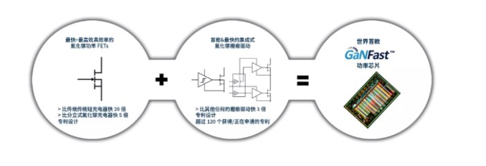
What is a GaN power chip?
Through SMT packaging, GaNFast™ GaN power chip realizes the integration of GaN device, drive, control and protection. These GaNFast™ power chips are an easy-to-use "digital in, power out" (digital in, power out) module. Since the impedance of the gate driver is basically zero, zero loss during turn-off can be achieved after integration. In addition, the opening performance can be customized and controlled according to specific application requirements.