ESP8266 IoT development board designTwo
Author: Teacher Zhang Jiao (Zhang Fei Senior Engineer of Actual Combat Electronics)
Hello everyone, today we continue the discussion of the schematic design part of the IoT development board.
In the previous article, we focused on the working process of the power supply, and as a whole determined the three power supply coordination methods: "flyback" + Buck + LDO. The flyback part is actually the adapter we bought, and we have decided to purchase this part through outsourcing. In this place, the LDO uses the AMS1117 solution, and its main task is to achieve a 5V to 3.3V step-down. Buck is the task of reducing the voltage from 12V to 5V.
You may have seen it elsewhere, using LDO solutions to reduce the voltage from 12V to 5V or 3.3V. There is a prerequisite for using this scheme, that is, the load cannot be too heavy, that is, the load current cannot be too large. If the load current is too large, the LDO DCDC chip will generate more heat. Because of the working principle of the LDO module, it still uses the nonlinear impedance (Rce) of a semiconductor device (such as T4 in the figure below) to step down. The greater the pressure difference, the greater the current, and the higher the power consumed on the LDO. Therefore, LDO is not suitable for large current and high voltage drop.

Then we must adopt a way of energy transfer with lower internal resistance, and the one we are more familiar with is the switching power supply. The more commonly used topological structure of step-down switching power supply is buck. Its principle is to use energy storage devices (capacitors, inductors) instead of energy-consuming devices (resistors) for energy transfer, so its energy efficiency ratio is very high. In addition, the use of switch on and off to adjust the energy transfer process, to achieve load dynamic adjustment and wide voltage input, for example, if the load is heavier, then the switch on time is longer, and the off time is shorter; if the load is After all, it is light, the time the switch is turned on is shorter, and the time it is turned off is longer.
The buck circuit of our development board is made with a DCDC chip, so that the size of the board can be smaller and more practical. If you want to fully understand the working principle of the buck circuit, you still have to find a way to build the power conversion circuit of the discrete device yourself, so that you can understand more deeply. As shown in the figure below, the chip used in our buck circuit is SY8120, and the idea of switch control is packaged inside the device.

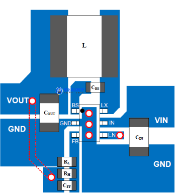
If you don't understand the working principle of this chip at once, you can find time to learn later. What I need to emphasize here is that for switching power supplies, the layout of the development board is very important. Because the switching signal is a step signal, it can be superimposed by expanding into a series of high-frequency Fourier series, that is, expanding into signals of various frequencies. But what we need is actually the fundamental signal, and other high-frequency things are interference for us. So when we are laying out, we must minimize the impact of these high-frequency signals on the outside, especially the Id part, so the Id loop should be as small as possible, one is to reduce the influence of the loop antenna to the outside The influence brought by the parasitic inductance of the trace on the road. Another, the +5V ground of the Buck power supply output must be grounded at a single point, because this ground is relatively dirty, and we must use a single-point grounding method to reduce its impact on other devices. In addition, during the layout, we try to keep the antenna part of the ESP-12F away from the buck circuit to further reduce the influence of the buck Id main circuit. The following figure is the layout reference given in the SY8120 datasheet. You can observe it, IN --- > LX --->L ---> Cout ---> GND This line, in fact, the loop has been as short as possible. Although the FB pin is also a high-frequency loop, its current is not large and is relatively not so important, so it is placed in a relatively secondary position. Attention everyone, here is only a relative term.
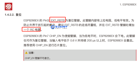
We also mentioned the reset circuit in the smallest system. So what is the specific reset process of the ESP8266 microcontroller we use? Let's take a look at the instructions related to the datasheet:
I just said that it would be fine to add an RC circuit outside, and at the same time put forward certain requirements for the wiring, and did not explain how the single-chip microcomputer resets. In fact, we only need to do as required. But we still have to find a way to deepen our understanding of the reset circuit as much as possible. We can refer to the reset circuit of the STM32F030 series single-chip microcomputer for comparison and understanding.
Let's take a look at the following two pictures, these two pictures illustrate the reset process when the microcontroller is powered on.


Let's take a look at the waveform of the Reset signal. When the power is turned on, the time that Reset remains low can be divided into two sections. The first period is the time from the VCC potential to the POR potential, and the second period is the time of Reset temporization. It is relatively easy to understand for the first time, can the microcontroller work only when the voltage is stable? In the second period, Reset temporization, most of the time during this period should be the time when the crystal oscillator starts to oscillate, as well as the time when other devices are reset. We have done a Reset test. The time from power-on to when a pin outputs a high level (this is the first line of the program). In STM32 F030, this time is about 2ms. Specifically, is the power-on reset of the ESP8266 film such a process? I think it is probably. No more material support has been found yet.
Let's take a look at the description of the button reset of the STM32F030 microcontroller.


You can take a look. The product documentation does not describe the reset time of the button. It just says that the voltage should be reduced to a certain level, for example, the voltage should be reduced to 0.8V. In this case, the RC designed by our circuit actually plays a filtering role, right, to prevent external interference from resetting the microcontroller. Let’s see if this function is the same as ESP8266’s description of the external resistance-capacitance circuit. So I speculate that the reset process of ESP8266 is similar to that of STM32F030 (not packed here). If you have more detailed information, you can study it further.

Specific to the value of R and C in the external resistance-capacitance circuit, we generally take the value R=10K, C=104. From the above analysis, it should be no problem to go to other values here. You can choose according to your actual situation (such as not too many types of BOM devices).
Let's take a look at how the crystal oscillator starts to oscillate. Because the module has already packaged the crystal oscillator inside, we don't have to worry about the design of the crystal oscillator part of the circuit. But in fact, the design of the crystal oscillator circuit is very important. After all, the crystal oscillator is the heartbeat of the single-chip microcomputer. How does the single-chip microcomputer work without a heartbeat signal? In addition, the design of the crystal oscillator circuit is also used in our USB-to-serial circuit, so I still plan to spend some time to explain the working principle of the crystal oscillator and some design points to everyone.


As shown in the picture above, there are actually a lot of things integrated under this iron cover, including a 26Mhz crystal. It's just that we can't see it because it's been encapsulated. Just like we mentioned earlier, it doesn't mean that it doesn't exist, right, haha. Due to space limitations, this article will stop here first. In the next article, we will focus on the analysis of the crystal oscillator's starting process and the design of peripheral circuits such as relays and temperature sensors.
Reference
(Copy the link to open in the browser)
① Passive crystal oscillator start-up conditions and its working principle http://m.elecfans.com/article/582154.html
②What is the principle of 51 single chip microcomputer crystal oscillator circuit?
https://www.zhihu.com/question/30930577/answer/55822425
③ Detailed explanation of three-point LC sine wave oscillation circuit
https://blog.csdn.net/weixin_42415539/article/details/88540709
④The waveform problem of capacitor three-point oscillating circuit
http://bbs.eeworld.com.cn/thread-1090538-1-1.html#pid2904297
⑤The working principle of the three-point capacitor oscillation circuit
https://zhuanlan.zhihu.com/p/354627295
⑥Single-chip power-on reset time https://blog.csdn.net/zyboy2000/article/details/4673955
⑦ESP8266 Document Center
https://docs.ai-thinker.com/esp8266/docs